

Key Words: Silicon Wafer Dicing PCB Depaneling Glass Cutting
Home > News > Industry News
【Description】:
An in-depth explanation of micron-level precision in glass laser cutting, covering tolerances, edge quality, positioning accuracy, and industrial applications.
A micron (also called a micrometre) is one‑millionth of a metre—0.001 millimetres. To put this in perspective, a human hair is approximately 50–100 microns thick. A typical sheet of paper is about 100 microns thick. The wavelength of visible light ranges from about 0.4 to 0.7 microns.
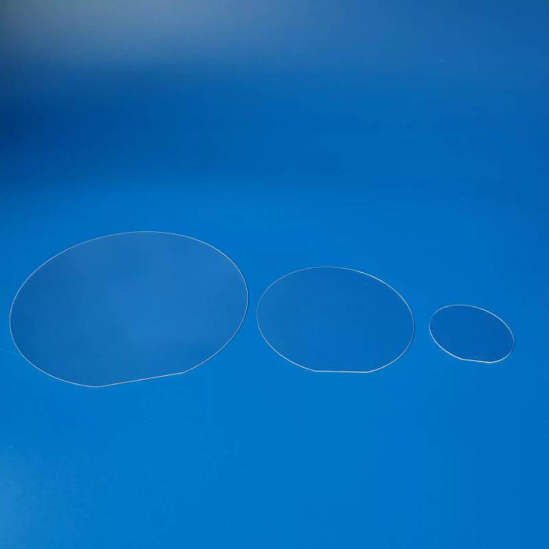
In micro-level glass cutting, features measured in microns are invisible to the naked eye but have profound effects on component performance:
| Feature | Typical Dimension | What It Affects |
|---|---|---|
| Edge roughness (Ra) | <0.5 µm | Optical clarity, sealing, bonding strength |
| Edge chipping | <5–10 µm | Mechanical strength, fold durability |
| Micro‑cracks | <1–5 µm (width) | Edge strength, reliability under stress |
| Positional deviation | ±2–5 µm | Assembly fit, registration with other components |
| Kerf width | 10–50 µm | Material utilisation, part density |
A deviation of just 5 microns—thinner than a human hair—can be the difference between a display that seals properly and one that fails. A micro‑crack of 1 micron can propagate under folding stress, reducing fold endurance from over 200,000 cycles to well below 50,000 cycles.
The term “micron‑level” encompasses multiple, distinct attributes of the cutting process. A process that delivers micron‑level precision must achieve the following:
This is the most straightforward aspect of micron‑level cutting: the ability to place the cut exactly where it is intended. Positioning accuracy of ±2–5 microns is typical for high‑precision glass cutting systems.
Why it matters: In display manufacturing, cuts must align precisely with deposited layers—TFT arrays, OLED pixels, and sealing lines. In semiconductor packaging, via positions must match pad locations. Even a deviation of a few microns can cause misregistration, leading to device failure.
Positional accuracy is meaningless if the cut edge itself is flawed. Micron‑level edge quality requires:
Edge roughness (Ra) below 0.5 microns: Ensures that the edge is smooth enough for optical clarity, reliable sealing, and consistent bonding.
Edge chipping below 5 microns: Ideally, no visible chipping at all. Any chip is a stress raiser.
No micro‑cracks: Subsurface cracks, even those too small to be seen optically, are unacceptable.
Thermal damage is measured in microns. For precision applications, the heat‑affected zone must be less than 2 microns—effectively negligible. Anything larger compromises edge strength and material integrity.
It is not enough to achieve precision once—it must be repeatable. Repeatability of ±2 microns ensures that the hundredth part is as accurate as the first. This is essential for high‑volume manufacturing.
Glass panels are not perfectly flat. Warpage, thickness variations, and mounting imperfections mean that the surface height varies across the panel. To achieve micron‑level precision across the entire panel, the system must compensate for these variations—typically through dynamic focus tracking.
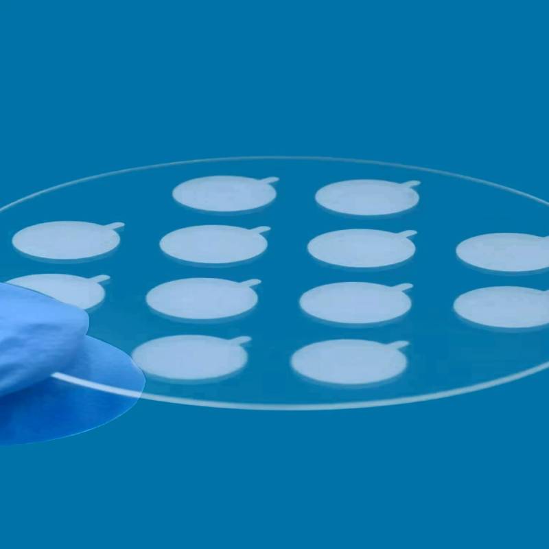
Micron‑level precision is a quantitative specification, not an absolute. It does not mean zero defects or unlimited capability. It means predictable, measurable, and repeatable performance within defined tolerances.
Some processes achieve a narrow kerf but produce rough edges with micro‑cracks. A narrow kerf is useful for material utilisation, but it is only one of several requirements for micron‑level precision.
High throughput is valuable for production, but it is not a measure of precision. A process may be fast but imprecise. Micron‑level precision requires controlled, consistent processing—speed without precision is wasteful.
The difference between 10 microns and 2 microns is significant in practice, even though both are “small”. A process that delivers 10‑micron positioning accuracy may be acceptable for some applications, but it should not be described as micron‑level precision. The threshold matters.
Some processes are described as “cold” or “thermal‑free”, but only picosecond and femtosecond lasers deliver true cold ablation. Nanosecond lasers have a measurable thermal component. Describing nanosecond processing as “cold” conflates different physical mechanisms. This distinction is critical for applications requiring the highest edge quality.
In OLED and LCD production, micron‑level precision ensures clean edges that enable reliable hermetic sealing. Any edge defect can compromise the seal, allowing moisture and oxygen to penetrate and degrade the display.
In UTG cutting, micron‑level precision—specifically, the elimination of micro‑cracks—is what enables fold endurance of over 200,000 cycles. Without micron‑level edge quality, foldable devices would fail within weeks of use.
In optical glass cutting, edge roughness below 0.5 microns ensures that light passes through without scattering. Any roughness degrades optical performance, reducing clarity and transmission.
In TGV drilling, micron‑level precision ensures that vias are placed accurately, with smooth sidewalls that enable consistent metal filling. Without this precision, via resistance increases, and electrical performance suffers.
In microfluidics, micron‑level precision ensures that fluid channels have consistent dimensions, enabling reliable flow and accurate diagnostics. Any variation can disrupt device performance.
| Element | Requirement |
|---|---|
| Laser source | UV picosecond (<10 ps) – cold ablation |
| Wavelength | UV (355 nm) – absorbed by glass |
| Beam quality | M² <1.3 – tight focus |
| Motion system | ±2–5 µm accuracy, ±2 µm repeatability |
| Focus control | Dynamic Z‑tracking – compensates for warpage |
| Process control | Optimised parameters – material‑specific |
| Environmental control | Thermal stability, vibration isolation |
| Cleanliness | Nitrogen assist + vacuum extraction |
Chanxan Laser provides the UV picosecond laser systems that deliver genuine micron‑level precision. The ultrafast laser system offers the combination of cold ablation, high beam quality, precision motion control, and clean processing that defines true micron‑level capability—enabling the advanced glass components that modern technology demands.

| Free solution
Previous: UV vs IR Laser for Precision Glass Cutting – A Complete Comparison
Next: How to Achieve Micron-Level Precision in Glass Laser Cutting- A Practical Guide







